LaserWand
Player controller — UWB tag, IMU, laser tip, retro bands.
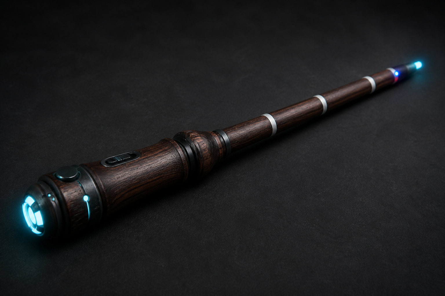
Wand hardware — layout & markers
Matches wand_sw/main/wand_config.h. Button is GPIO15 active-low
(switch to GND, MCU pull-up). Optical tracking = passive retroreflective tape
on the shaft (zero electronics).
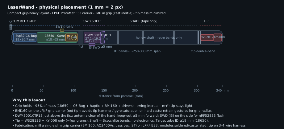
Electronics (grip-heavy prototype) hw pending
- Grip: Esp32-C6-Bug, 18650, USB-C pommel, LPKF carrier (BMI160, AO3400As, haptic, SW1 GPIO15 active-low)
- UWB shelf (above fist): DWM3001CTR13 (UART), antenna toward tip, ≥5 mm keep-out; J3 SWD
- Tip: KY-008 laser + WS2812 RGB VFX only
- Shaft: Scotchlite-class retro bands only — no electronics
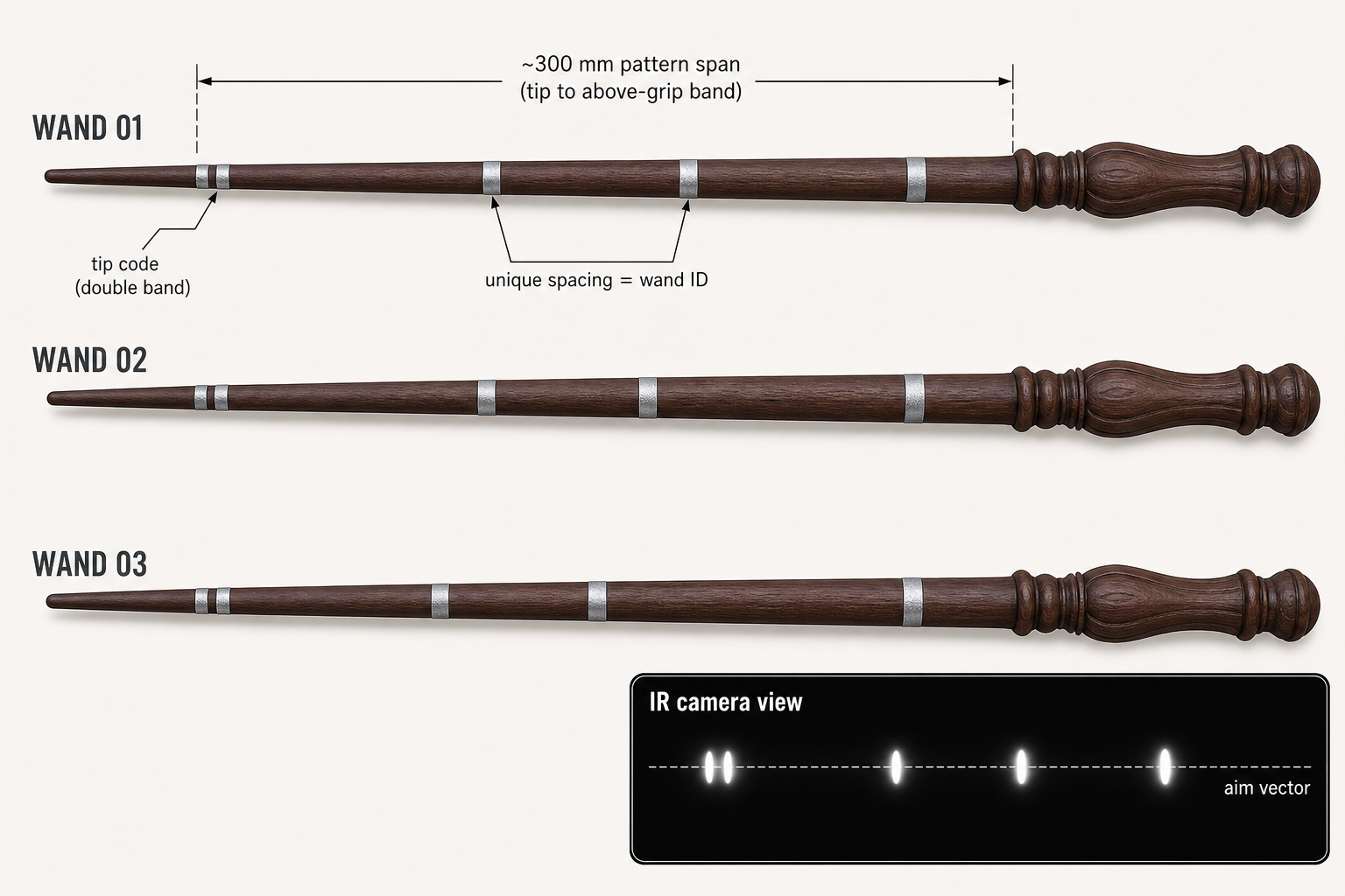
Optical markers (v2)
- Passive Scotchlite bands — applied with fleet spacing jig
- Ceiling: OV9281 + continuous 850 nm illuminator (v2 only)
- Coloured grip wrap = staff ID only (cameras are mono IR)
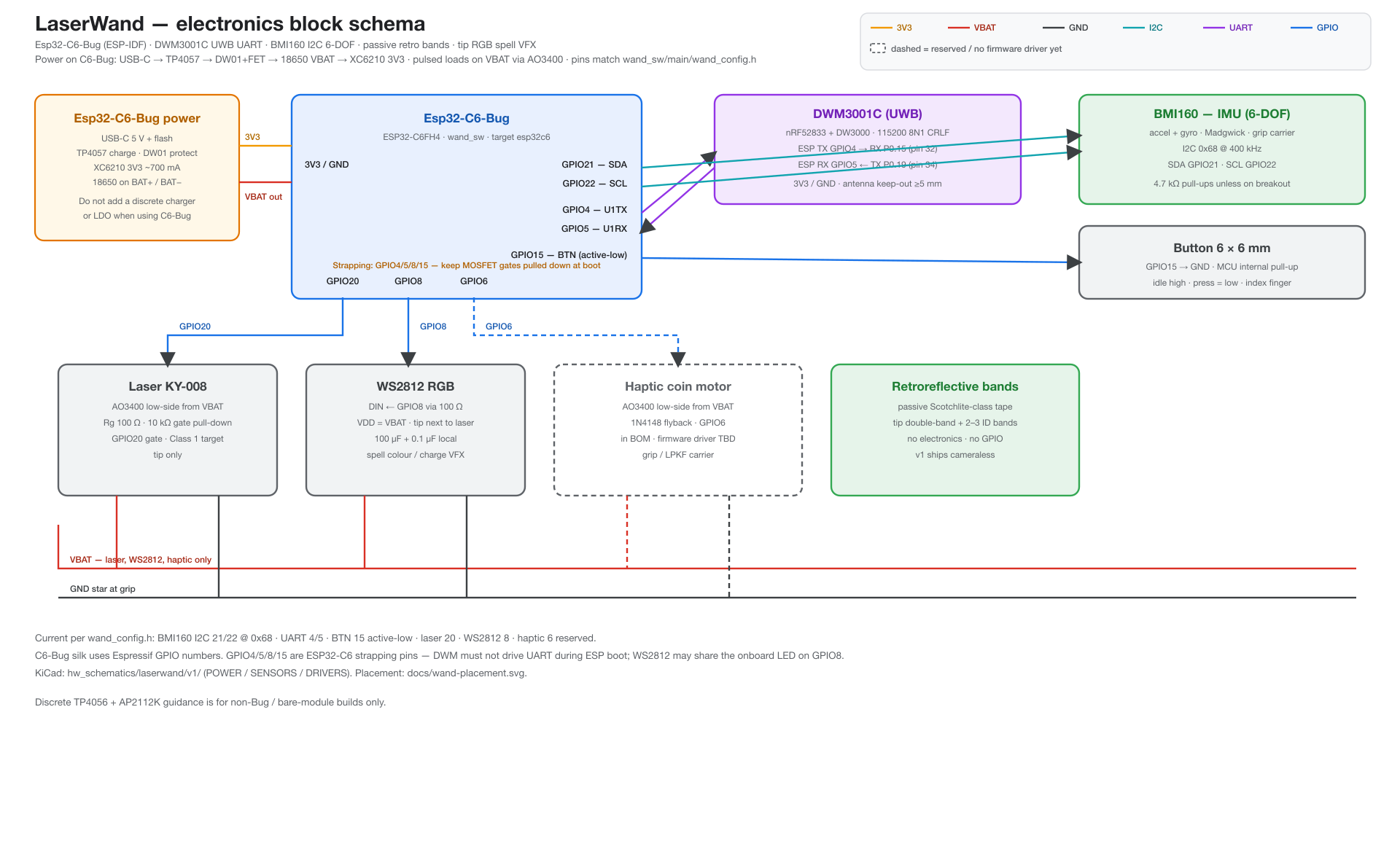
wand_config.h).
Optical path = passive retro bands.
C6-Bug integrates charge / protect / 3V3. Vector companion: wand-electronics-overview.svg.DWM3001C — pinout, J-Link, UART
Same Qorvo module on the wand and every anchor. The ESP32-C6 talks to it over UART (115200 8N1, CRLF). The on-module nRF52833 is programmed over SWD from a SEGGER J-Link 10-pin socket. Canonical write-up: HARDWARE.md.
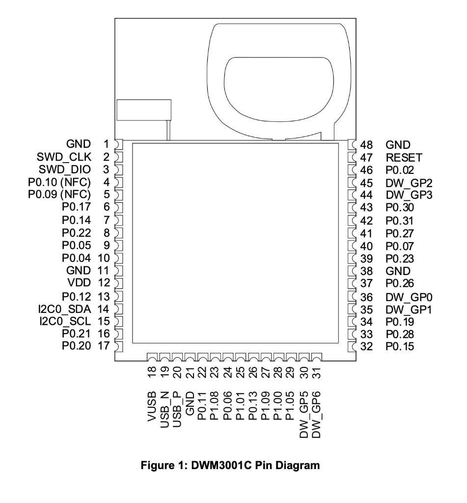
J-Link 10-pin socket · pin face
The programmer cable is a 10-pin header in two rows of five. Only five wires are used; unused holes stay open. Socket pin 1 is top-left (key notch on that side).
cd DWM3001C-starter-firmware-main && make build && make flash — see RUNBOOK A2.UART — ESP32-C6 ↔ DWM
Cross-wired. Firmware: custom_board.h RX_PIN_NUMBER=15, TX_PIN_NUMBER=19.
| ESP32-C6 | DWM3001C | nRF |
|---|---|---|
| TX GPIO 4 | pin 32 UWB RX | P0.15 |
| RX GPIO 5 | pin 34 UWB TX | P0.19 |
| GND | GND | — |
ESP GPIO 4 / 5 — not DWM pin 3 (SWD_DIO) or DevKit header positions 3 / 4.
Why those pads
Pins 32 and 34 sit on the right edge of the figure, just above the bottom corner — generic P0.15 / P0.19 labels, not “TX/RX”.
The DW3000 radio is driven inside the module firmware; the ESP never speaks SPI to it.
Same UART pins on wand (wand_config.h) and anchor (anchor_sw/main/main.c UART1).
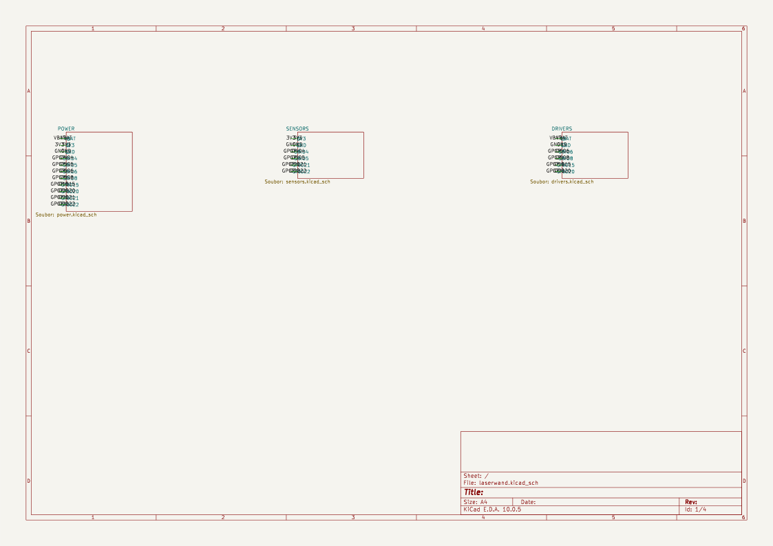
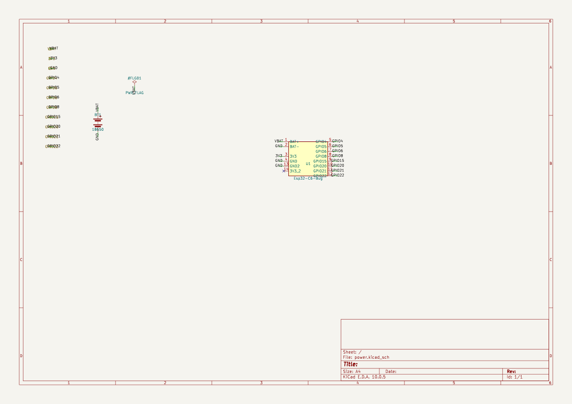
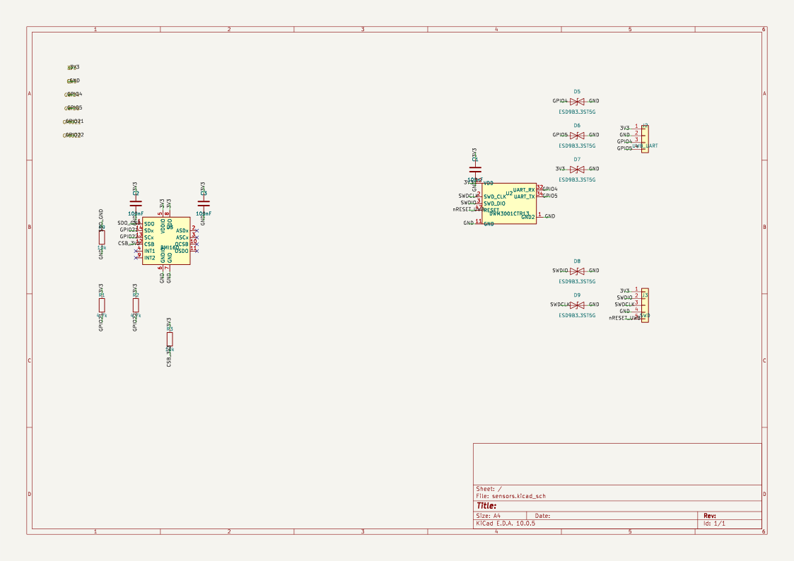
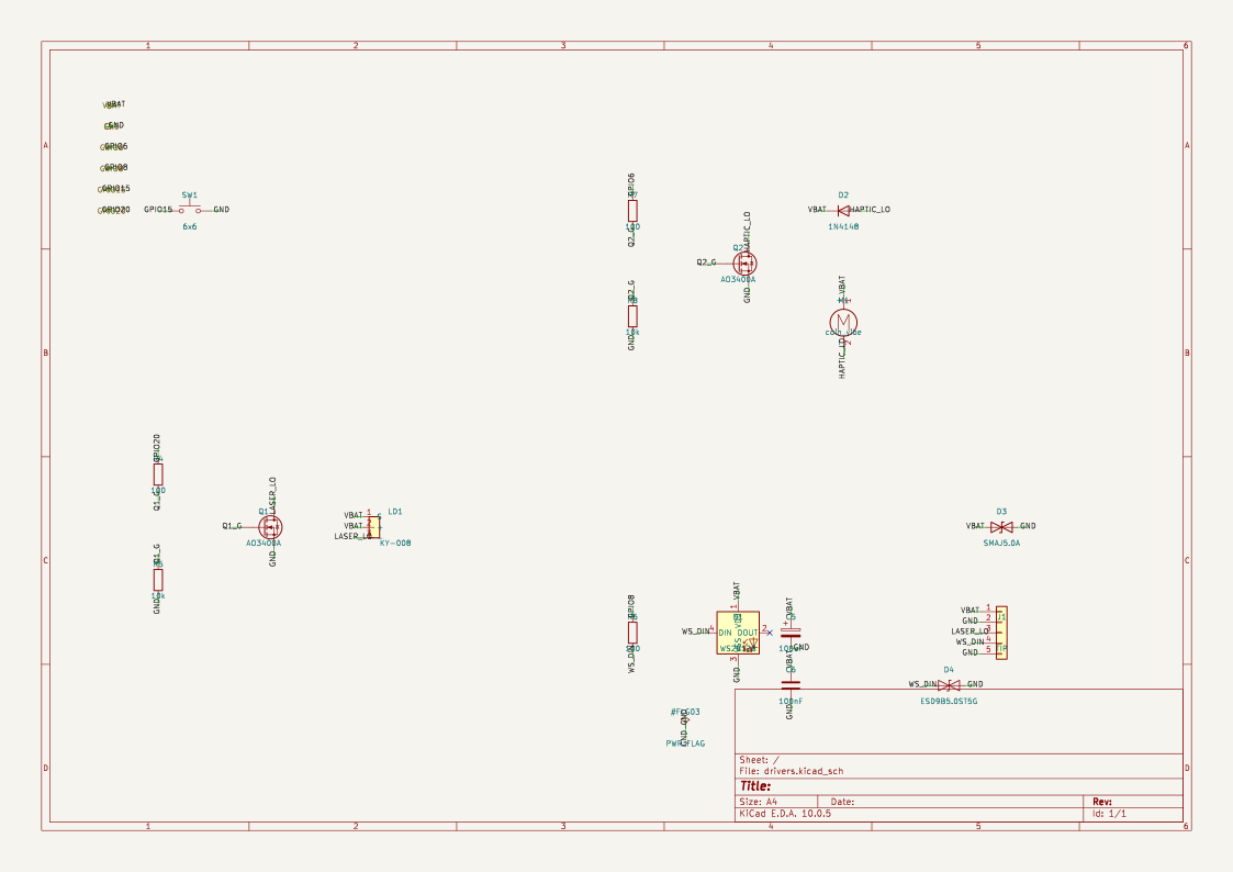
Circuit schematic hw pending
Hierarchical KiCad design under hw_schematics/laserwand/v1/.
Four sheets: root hierarchy, POWER, SENSORS, DRIVERS.
Wand build — placement rationale & soldering guide hw pending
Why every part sits where it sits, and how to solder/assemble the wand so it
survives being swung all day. Full engineering detail lives in
docs/WAND_BEST_PRACTICES.md — this is the field summary.
Esp32-C6-Bug integrates USB-C charging, cell protection, and 3V3 regulation; the discrete TP4056 + DW01/FS8205 + AP2112K guidance applies only to non-Bug / bare-module builds.
Placement — the physics of a swung stick
Mass lives in the grip
A wand pivots at the wrist; the effective swing weight of a part grows with the square of its distance from the pivot. Grams at the tip feel like a hammer, grams in the grip are nearly free. So the 18650 cell and control boards sit in the grip, and the tip carries only what must be there.
Discrete charger: next to USB-C, beside the cell
For non-Bug / bare-module builds, USB-C → TP4056 → 18650 is the highest-DC-current loop in the wand (up to ~1 A at the default Rprog; the sealed tube prefers 0.5 A — Rprog ≈ 2.4 kΩ — for less heat). Keeping the three adjacent at the pommel means short fat traces, no charge current routed down the shaft, less heat and noise near the emitters. Leave a few mm air gap between the charger and the cell wall — the linear TP4056 warms up while charging and Li-ion likes staying cool. The module must carry the DW01 + FS8205 protection pair (B+/B− pads).
IMU on the LPKF grip carrier
BMI160 lives in the grip with the mass stack — not at the tip. Hard casts no longer hammer the gyro at full lever arm; swing inertia stays low. Retrain gesture models for grip radius (tip-trained TFLite models will not transfer cleanly). Mount rigidly on the carrier, axes aligned with the shaft.
UWB shelf just above the fist
DWM3001CTR13 sits on a shelf immediately above the fist so the antenna clears the hand without putting mass at the tip. Keep a ≥5 mm keep-out forward of the antenna. The 18650 sits immediately aft of the UWB shelf and must not shadow or cross the antenna face; no battery wires across it either. J3 SWD on the side for nRF52833 flash. Antenna end toward the tip.
Retro bands define the aim vector (v2 optical)
Apply 3–4 Scotchlite tape bands over ~250–300 mm using a fleet spacing jig. Tip double band marks orientation; unique spacing = wand ID. Bands wrap fully around the shaft (visible from any roll). No solder, no MOSFETs, no sync. Optional coloured grip wrap for staff ID only (cameras are mono IR). v1 ships without cameras — bands are cheap future-proofing.
Emitters & button
The tip contains only the laser + forward RGB / WS2812 (spell colour only); its harness is VBAT/GND + laser gate + WS2812 data, with no I²C trunk to the tip. Button on grip → GPIO15 active-low with internal pull-up (switch-to-GND).
Soldering — the rules that matter
Wire gauge by net
- VBAT / GND trunk (battery → regulator): 24–22 AWG
- Laser / WS2812 feed: 26–24 AWG, kept short
- Signals (I²C, UART, GPIO, WS2812 data): 30–28 AWG
- Colour code: red VBAT, black GND, yellow 3V3, then signals.
Route power and signals apart
- Keep I²C in the grip; route the tip harness as VBAT/GND + laser gate + WS2812 data only.
- Keep signals away from the laser/WS2812 feed; cross at 90° if needed.
- WS2812 data: ~100 Ω series at the source end.
- GND star at the grip — don't daisy-chain grounds through modules.
Decoupling
- 100 µF + 0.1 µF at WS2812 / laser feed if needed.
- 0.1 µF ceramic close to BMI160 VDD.
- Retro bands are passive — zero tracking power on the wand.
Laser / optional haptic
- Laser on GPIO20 (Class 1 — KY-008 attenuated to Class 1 AEL).
- Haptic (GPIO 6 reserved): MOSFET + flyback diode if added.
Solder technique
- Leaded 63/37 at ~330 °C, 1–2 s per joint; add flux, don't cook flux out.
- Tin wire and pad first, then join — no "blob and hope".
- Joint must be shiny and concave; grey/ball = cold joint, redo it.
- Heat-shrink every splice (no bare tape); kapton over anything facing the cell.
Assembly & bring-up order
- Bench-test every module loose before anything enters the tube: flash ESP32-C6, talk to DWM3001CTR13 over UART (115200 8N1, CRLF), read BMI160 (0x68), blink WS2812.
- Power chain first, alone: verify Esp32-C6-Bug's integrated USB-C charge/protection/3V3 path. For non-Bug / bare-module builds, verify USB-C → TP4056 → protected cell → AP2112K-3.3, ≥600 mA (MCP1700 is undersized for WiFi + UWB peaks). Verify charge indication, charge termination, and 3.3 V under load before connecting any logic.
- Harness on the bench, full length, connectors on — test everything joined but outside the shell. Fix it now, not through a 15 mm hole.
- Slide in tip-first, anchor the emitter harness as you go; then seat the grip-carrier IMU rigidly and respect the UWB antenna keep-out. Align button and USB-C last.
- Apply retro bands from fleet jig; QC photo under bench IR camera (optional before v2).
- Re-run self-test after closing: I²C scan, UWB ranging, IMU stream, charge cycle. Label wand ID.